- 您现在的位置:买卖IC网 > Sheet目录2000 > IDT82V3355EDG (IDT, Integrated Device Technology Inc)IC PLL WAN SYNC ETHERNET 64TQFP
IDT82V3355
SYNCHRONOUS ETHERNET WAN PLL
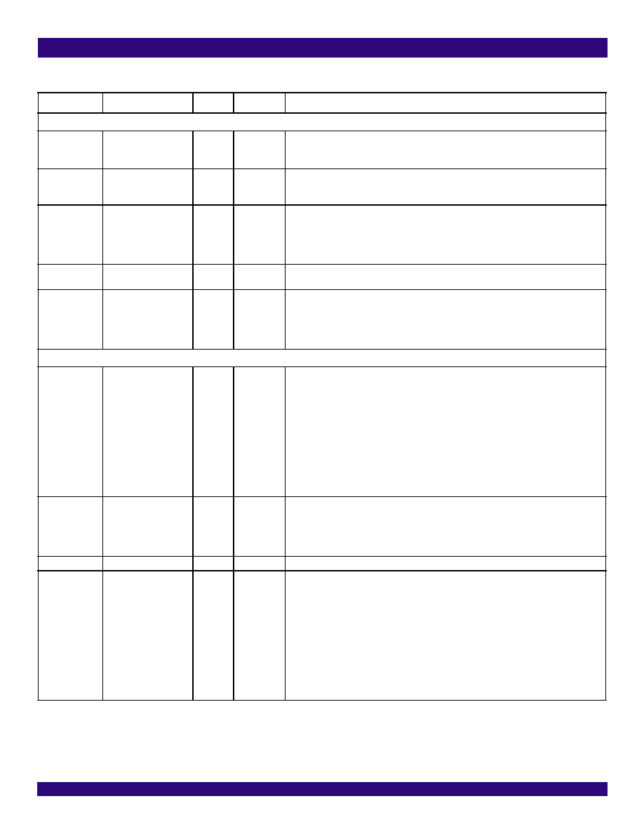
Pin Description
15
May 19, 2009
JTAG (per IEEE 1149.1)
TRST
37
I
pull-down
CMOS
TRST: JTAG Test Reset (Active Low)
A low signal on this pin resets the JTAG test port.
This pin should be connected to ground when JTAG is not used.
TMS
41
I
pull-up
CMOS
TMS: JTAG Test Mode Select
The signal on this pin controls the JTAG test performance and is sampled on the rising edge
of TCK.
TCK
49
I
pull-down
CMOS
TCK: JTAG Test Clock
The clock for the JTAG test is input on this pin. TDI and TMS are sampled on the rising edge
of TCK and TDO is updated on the falling edge of TCK.
If TCK is idle at a low level, all stored-state devices contained in the test logic will indefinitely
retain their state.
TDI
51
I
pull-up
CMOS
TDI: JTAG Test Data Input
The test data is input on this pin. It is clocked into the device on the rising edge of TCK.
TDO
50
O
CMOS
TDO: JTAG Test Data Output
The test data is output on this pin. It is clocked out of the device on the falling edge of TCK.
TDO pin outputs a high impedance signal except during the process of data scanning.
This pin can indicate the interrupt of T0 selected input clock fail, as determined by the
LOS_FLAG_ON_TDO bit (b6, 0BH). Refer to Chapter 3.8.1 Input Clock Validity for details.
Power & Ground
VDDD1
VDDD2
VDDD3
VDDD4
VDDD5
VDDD6
8
12
9
32
36, 38, 39, 45, 46
54
Power
-
VDDDn: 3.3 V Digital Power Supply
Each VDDDn should be paralleled with ground through a 0.1 F capacitor.
VDDA1
VDDA2
VDDA3
4
14
57
Power
-
VDDAn: 3.3 V Analog Power Supply
Each VDDAn should be paralleled with ground through a 0.1 F capacitor.
VDD_DIFF
22
Power
-
VDD_DIFF: 3.3 V Power Supply for OUT1
DGND1
DGND2
DGND3
DGND4
DGND5
DGND6
7
11
10
31
40
53
Ground
-
DGNDn: Digital Ground
Table 1: Pin Description (Continued)
Name
Pin No.
I/O
Type
Description 1
发布紧急采购,3分钟左右您将得到回复。
相关PDF资料
IDT82V3358EDG
IC PLL WAN SYNC ETHERNET 64TQFP
IDTCSPT857DNLG8
IC PLL CLK DVR SDRAM 40-VFQFPN
IDTCV105EPVG8
IC CLK GEN DESKTOP PC 48-SSOP
IDTCV110NPVG
IC FLEXPC CLK PROGR P4 56-SSOP
IDTCV115-2PVG
IC FLEXPC CLK PROGR P4 56-TSSOP
IDTCV115FPVG
IC FLEXPC CLK PROGR P4 56-SSOP
IDTCV119EPVG8
IC CLK GEN DESKTOP PC 48-SSOP
IDTCV133PAG
IC FLEXPC CLK PROGR P4 56-TSSOP
相关代理商/技术参数
IDT82V3355EDG8
制造商:Integrated Device Technology Inc 功能描述:IC PLL WAN SYNC ETHERNET 64TQFP
IDT82V3355EDGBLANK
制造商:IDT 制造商全称:Integrated Device Technology 功能描述:SYNCHRONOUS ETHERNET WAN PLL
IDT82V3355TFBLANK
制造商:IDT 制造商全称:Integrated Device Technology 功能描述:SYNCHRONOUS ETHERNET WAN PLL
IDT82V3355TFG
功能描述:IC PLL WAN SYNC ETH 64-TQFP RoHS:是 类别:集成电路 (IC) >> 时钟/计时 - 专用 系列:- 标准包装:1,500 系列:- 类型:时钟缓冲器/驱动器 PLL:是 主要目的:- 输入:- 输出:- 电路数:- 比率 - 输入:输出:- 差分 - 输入:输出:- 频率 - 最大:- 电源电压:3.3V 工作温度:0°C ~ 70°C 安装类型:表面贴装 封装/外壳:28-SSOP(0.209",5.30mm 宽) 供应商设备封装:28-SSOP 包装:带卷 (TR) 其它名称:93786AFT
IDT82V3355TFG8
功能描述:IC PLL WAN SYNC ETH 64-TQFP RoHS:是 类别:集成电路 (IC) >> 时钟/计时 - 专用 系列:- 标准包装:1,500 系列:- 类型:时钟缓冲器/驱动器 PLL:是 主要目的:- 输入:- 输出:- 电路数:- 比率 - 输入:输出:- 差分 - 输入:输出:- 频率 - 最大:- 电源电压:3.3V 工作温度:0°C ~ 70°C 安装类型:表面贴装 封装/外壳:28-SSOP(0.209",5.30mm 宽) 供应商设备封装:28-SSOP 包装:带卷 (TR) 其它名称:93786AFT
IDT82V3355TFGBLANK
制造商:IDT 制造商全称:Integrated Device Technology 功能描述:SYNCHRONOUS ETHERNET WAN PLL
IDT82V3358
制造商:IDT 制造商全称:Integrated Device Technology 功能描述:SYNCHRONOUS ETHERNET WAN PLL
IDT82V3358EDG
功能描述:IC PLL WAN SYNC ETHERNET 64TQFP RoHS:是 类别:集成电路 (IC) >> 时钟/计时 - 专用 系列:- 标准包装:1,500 系列:- 类型:时钟缓冲器/驱动器 PLL:是 主要目的:- 输入:- 输出:- 电路数:- 比率 - 输入:输出:- 差分 - 输入:输出:- 频率 - 最大:- 电源电压:3.3V 工作温度:0°C ~ 70°C 安装类型:表面贴装 封装/外壳:28-SSOP(0.209",5.30mm 宽) 供应商设备封装:28-SSOP 包装:带卷 (TR) 其它名称:93786AFT